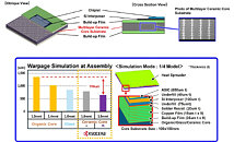
Kyocera Corporation (President: Shiro Sakushima; "Kyocera") today announced that it is commercializing a new multilayer ceramic core substrate for advanced semiconductor packages, such as xPUs and switch ASICs, which are rapidly scaling in complexity as AI data center architectures evolve. The new product will be unveiled at ECTC 2026, an international conference on semiconductor packaging technologies, in Orlando, Florida, USA, May 26-29, 2026. Built from Kyocera's proprietary Fine Ceramic materials, the new core substrate is engineered for high‑density wiring and exceptional rigidity. According to the company, these characteristics dramatically reduce deformation (warpage) in high-performance semiconductor packages, a key challenge as demand for greater device integration and higher processing speed continues to rise.